| Features | SAB 2791 | SAB 2793 | SAB 2795 | SAB 2797 |
| Single Density (FM) | X | X | X | X |
| Double Density (MFM) | X | X | X | X |
| True Data Bus | X | X | ||
| Inverted Data Bus | X | X | ||
| Side Select Output | X | X | ||
| Internal CLK Divide | X | X |
SAB 279X is a floppy disk controller family of N-channel MOS LSI components designed to interface with SAB 8080/8085/8086/8051 family processors. Its flexibility and ease of use makes it an ideal floppy disk interface between conventional floppy disks and all computer systems. Software compatible with its predecessor, the SAB 179X, the device also contains a high performance Phase- Lock-Loop Data Separator as well as Write Precompensation Logic. When operating in Double Density Mode, Write Precompensation is automatically engaged to a value programmed via an external potentiometer. An on-chip VCO and phase comparator allows adjustable frequency range for 5Ľ"-8" Floppy Disk and Micro Floppy Disk interface.
The SAB 279X are N-channel MOS LSI devices which perform the functions of a Floppy Disk Formatter/Controller in a single chip implementation. The SAB 279X is IBM 3740 compatible in single density mode (FM) and System 34 compatible in Double Density Mode (MFM). The SAB 279X contains all the features of its predecessor, the SAB 179X, plus a high pertormance phase-lock-loop data separator as well as write precompensation logic. In double density mode, write precompensation is automatically engaged to a value programmed via an external potentiometer. In order to maintain compatibility, the SAB 179X and SAB 279X designs were made as close as possible with the computer interface, instruction set. and I/O registers being identical. Also. head load control is identical in each case, the actual pin assignments vary by only a few pins from any one to another.
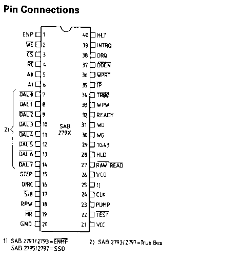
The processor interface consists of an 8-bit bi- directional bus for data, status, and control word transfers. The SAB 279X is set up to operate on a multiplexed bus wilh other bus-oriented devices. The SAB 279X is TTL compatible on all inputs and outputs. The outputs will drive one TTL load or three LS loads. The SAB 2793 is identical with the SAB 2791. except that the DAL lines are true for systems that utilize true data busses. The SAB 2795/7 has a side select output for controlling double sided drives.
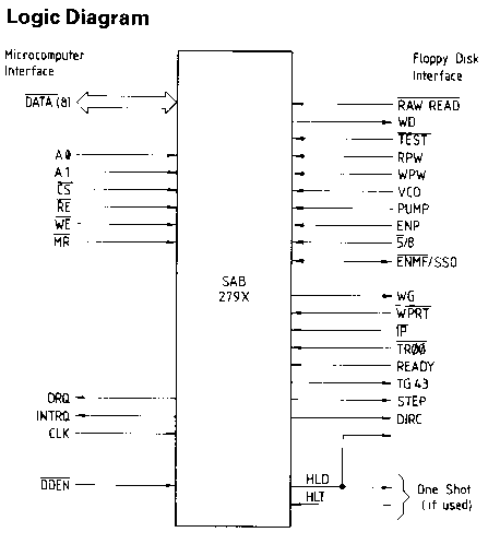
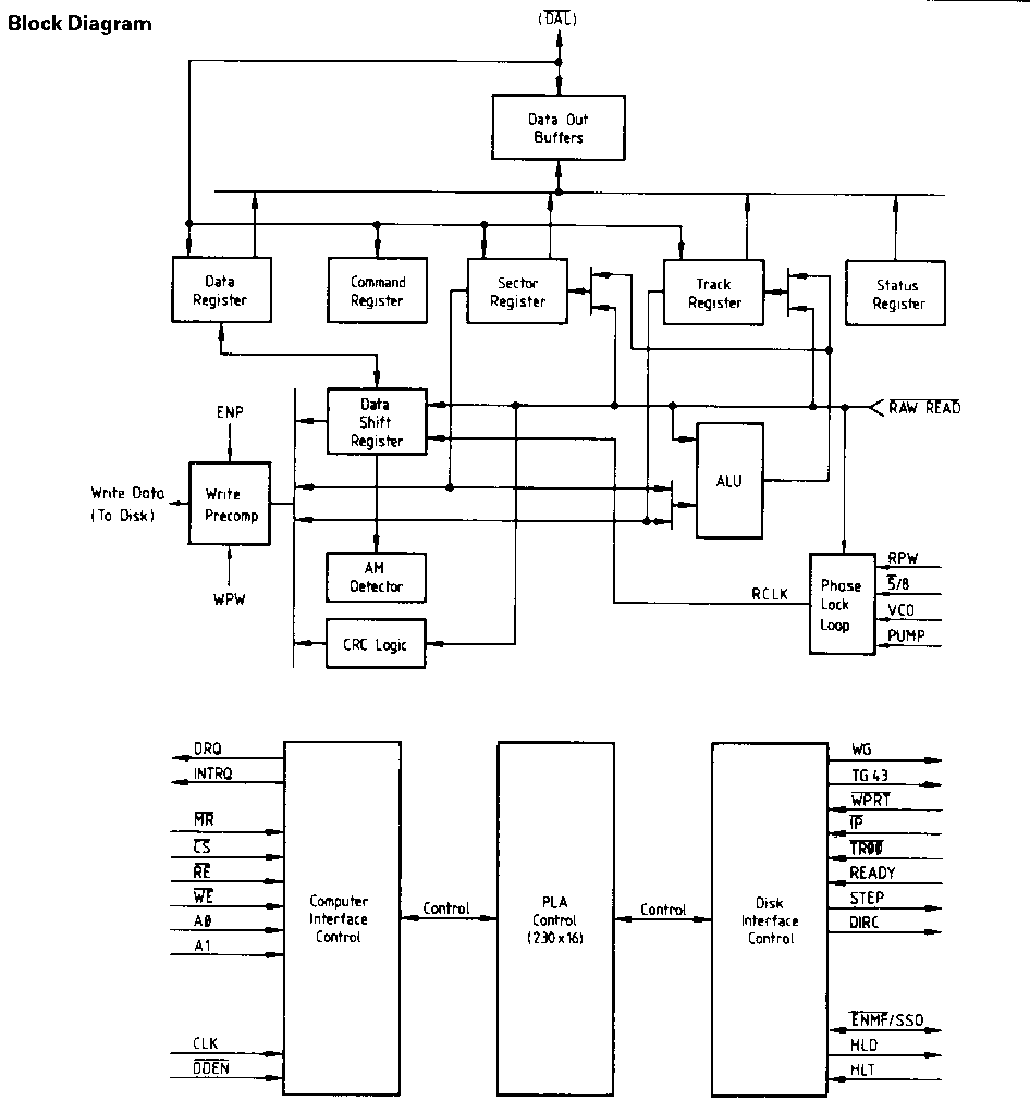
The Floppy Disk Formatter block diagram is illustrated on page 5. The primary sections include the parallel processor interface and the Floppy Disk interface.
Data Shift Register (DSR) - This 8-bit register assembles serial data from the Read Data input (RAW READ) during read operations and transfers serial data to the Write Data output during write operations.
Data Register (DR) - This 8-bit register is used as a holding register during disk read and write operations. In disk read operations the assembled data byte is transferred in parallel to the Data Register from the Data Shift Register. In disk write operations information is transferred in parallel from the Data Register to the Data Shift Register. When executing the Seek command the Data Register holds the address of the desired track position. This register is loaded from the DAL and gated on to the DAL under processor control.
Track Register (TR) - This 8-bit register holds the track number of the current Read/Write head position. It is incremented by one every time the head is stepped in (towards track 76) and decremented by one when the head is stepped out (towards track 00). The contents of the register are compared with the recorded track number in the ID field during disk read, write and veriy operations. The Track Register can be loaded from or transferred to the DAL. This register should not be loaded when the device is busy.
Sector Register (SR) - This 8-bit register holds the address of the desired sector position. The contents of the register are compared with the recorded sector number in the ID field during disk read or write operations. The Sector Register contents can be loaded from or transferred to the DAL. This register should not be loaded when the device is busy.
Command Register (CR) - This 8-bit register holds the command presently being executed. This register should not be loaded when the device is busy unless the new command is a Force Interrupt command. The command register can be loaded from the DAL, but not read onto the DAL.
Status Register (STR) - This 8-bit register holds device status information. The meaning of the status bits is a function of the type of command previously executed. This register can be read onto the DAL, but not loaded from the DAL.
CRC Logic - This logic is used to check or to generate the 16-bit Cyclic Redundancy Check (CRC). The polynomial is: G(x) = x^16 + x^12 + x^5 + 1 The CRC includes all information starting with the address markund up to the CRC character. The CRC register is preset to ones prior to data being shifted through the circuit.
Arithmetic/Logic Unit (ALU) - The ALU is a serial comparator, incrementer, and decrementer and is used for register modification and comparisons with the disk recorded ID field.
Timing and Control - All computer and Floppy Disk interface controls are generated through this logic. The internal device timing is generated from an . external crystal clock.
AM Detector - The address mark detector detects ID, data and index address marks during read and write operations.
Write Precompansation - enables write precompensation to be performed on the Write Data output.
Data Separator - a high pertormance phase-lock- loop data separator with on-chip VCO and phase comparator allows adjustable frequency range for 5Ľ" or 8" Floppy Disk interfacing.
The interface to the processor is accomplished through the eight Data Access Lines (DAL) and associated control signals. The DAL are used to transfer data, status, and control words out of, or into the SAB 279X. The DAL are three state buffers that are enabled as output drivers when Chip Select (-CS) and Read Enable(-RE)are active (low logic state) or act as input receivers when -CS and Write Enable (-WE) are active.
When transfer or data with the Floppy Disk Controller
is required by the host processor, the device
address is decoded and -CS is made low. The address
bits A1 and A0, combined with the signals -RE
during a read operation or -WE during a write
operation are interpreted as selector for the following
registers:
A1  A$  REA0        WRITE
$   $   Status Register   CommandRegister
$   1   Track Register   Track Register
1   $   Sector Register   Sector Register
1   1   Oata Regisler    Oata Regisler
During direct memory access (DMA) types of data are transferred between the Data Register of the SAB 279X and the processor. the Data Request (DRQ) output is used in data transfer control. This signal also appears as status bit 1 during read and write operations.
In disk read operations the Data Request is activated (set high) when an assembled serial input byte is transterred in parallel to the Data Register. This bit is cleared when the Data Register is read by the processor. If the Data Register is read after one or more characters have been lost by having transferred new data into the register prior to processor readout, the Lost Data bit is set in the Status Register. The read operation continues until the end of sector is reached.
In disk write operations the Data Request is activated when the Data Register transfers its contents to the Data Shift Register, and requires a new data byte. It is reset when the Data Register is loaded with new data by the processor. If new data is not loaded at the time the next serial byte is required by the Floppy Disk, a byte of zeroes is written on the diskette and the Lost Data bit is set in the Status Register.
Upon completion ot every command an INTRQ is generated, INTRQ is reset either by reading the Status Register or by loading the Command Register with a new command. In addition, INTRQ is generated if a force Interrupt command condition is met.
The SAB 279X has two modes of operation depending on the state of -DDEN (Pin 37). When -DDEN = 1, Single Densitv (FM) is selected. When -DDEN = 0, Double Density (MFM) is selected. In either case, the CLK input (Pin 24) is set at 2 MHz tor 8" drives or 1 MHz for 5Ľ" drives.
On the SAB 2791/2793, the -ENMF input (Pin25) can be used for controlling both, 5Ľ" and 8" drives with a single 2 MHz clock. When -ENMF = 0, an internal divide by 2 of the CLK is performed. When -ENMF = 1, no divide takes place. This allows the use of a 2 MHz clock for both, 5Ľ" and 8" configurations.
The internal VCO trequency must also be set to the proper value. The -5/8 input (Pin 17) is used to select data separator operation by internally dividing the read clock. When -5/8 = 0, 5Ľ" data separation is selected; when -5/8 = 1, 8" drive data separation is selected.
| CLOCK (24) | -ENMF (25) | -5/8 (17) | DRIVE |
| 2 MHz | 1 | 1 | 8" |
| 2 MHz | 0 | 0 | 5Ľ" |
| 1 MHz | 1 | 0 | 5Ľ" |
The SAB 279X is software compatible with the SAB 179X series of floppy Disk Controllers. Commands, status, and data transfers are performed in the same way. Software generated for the SAB 179X can be transferred to a SAB 279X system without modification.
In addition to the SAB 179X, the SAB 219X contains an internal data separator and write precompensation circuit. The TEST (Pin 22) line is used to adjust both, data separator and precompensation. When -TEST = 0, the WD (Pin 31) line is internally connected to the output of the write precomp single shot. Adjustment of the WPW (Pin 33) line can then be accomplished. A second single shot tracks the precomp setting at approximately 3:1 to ensure adequate Write Data pulse widths to meet drive specifications.
Similarly, data separation is also adjusted with -TEST - 0. The TG43 (Pin 29) line is internally connected to the output of the read data single shot, which is adjusted via the RPW (Pin 18) line. The DIRC (Pin 16) line contains the read clock output (5OO kHz for 8" drives). The VCO trimming capacitor (Pin 26) is adjusted to center frequency.
Internal timing signals are used lo generate pulses during the adjustment mode so that these adjustments can be made while the device is in operation. The -TEST line also contains a pull-up resistor, so adjustments can be performed simply by grounding the -TEST pin, overriding the pull-up. The -TEST pin cannot be used to disable stepping rates during operation as its function is quite different from the SAB 179X.
Other pins on the device also include pull-up resistors and mav be left open to satisfy a logic 1 condition. These are: ENP, -5/8, -ENMF, -WPRT, -DDEN, HLT, =TEST, and -MR.
Sector lengths of 128, 256, 512 or 1024 are obtainable either in FM or MFM formats. For FM, -DDEN should be placed to logic 1. For MFM formats, -DDEN should be placed to a logic 1. Sector lengths are determined at format time by the fourth byte in the ID field.
Sector Length Table*
| Sector Length Field(hex) |
Number of Bytes in Sector (decimal) |
| 00 | 128 |
| 01 | 256 |
| 02 | 512 |
| 03 | 1024 |
The number ot sectors per track as far as the SAB 279X is concerned can be from 1 to 255 sectors. The number of tracks as far as the SAB 279X is concerned is from 0 to 255 tracks. For IBM 3740 compatibility, sector lengths are 128 bytes with 26 sectors per track. For System 34 compatibilily (MFM), sector lengths are 256 bytes/sector with 26 sectors/track; or lengths of 1024 bytes/sector with 8 sectors/track.
When writing is to take place on the diskette the Write Gate (WG) output is activated, allowing current to flow into the Read/Write head. As a precaution to erroneous writing the first data byte must be loaded inlo the Data Register in response to a Data Request from the SAB 279X before the Write Gate signal can be activated.
Writing is inhibited when the Write Protect input is logic low, in which case any write command is immedialely terminated, an interrupt is generated and the Write Protect status bit is set.
for write operations, Ihe SAB 279X provides Write Gate (Pin 30) and Write Data (Pin 31) outputs. Write Data consists of a series of pulses set to a width approximately three times greater than the precomp adjustment. Write Data provides the unique address marks in both formats.
Whenever a read or write command (Type II or III) is received the SAB 279X samples the Ready input. If this input is logic low the command is not executed and an interrupt is generated. All Type I commands are performed regardless of the State of the Ready input. Also, whenever a Type II or III command is received, Ihe TG43 signal output is updated. TG 43 may be tied to ENP to enable write precompensation on tracks 44-76.
Setting the write precomp value is accomplished by forcing lhe -TEST line (Pin 22) to a logic 0. A stream of pulses can then be seen on the Write Data (Pin 31) line. Adjust the WPW Potentiometer for the desired pulse width. This adjustment may be performed in-circuit since Write Gate (Pin 30) is inactive while -TEST = 0.
The SAB 279X can operate with either an external data separator or its own internal recovery circuit. The condition of the -TEST line (Pin 22) in conjunction with -MR (Pin 19) will select internal or external mode.
To program the SAB 279X for external VCO, a -MR pulse must be applied while -TEST = 0. A clock equivalent to eight times the data rate (e.g., 4.O MHz for 8" double density) is applied lo the VCO input (Pin 26). The feedback reference voltage is available on the Pump output (Pin23) for external integration to control the VCO. -TEST is returned to a logic 1 for normal operation. Note: To maintain this mode, -TEST must be held low whenever -MR is applied. For internal VCO operation, the TEST line must be high during the -MR pulse, then set to a logic 0 for the adjustment procedure.
A 50 k Potentiameter tied to the RPW input (Pin 18) is used to set the internal Read Data pulse for proper phasing. With a scope on Pin 29 (TG43), adjust the RPW pulse for 1/8 of the data rate (250 ns for 8" Double Densily). An external variable capacitor of typically 5-60 pF is tied to the VCO input (Pin 26) for adjusting center frequency. With a frequency counter on Pin 16 (DIRC) adjust the trimmer cap to yield the appropriate data rate (500 kHz for 8" Double Density). The -DDEN line must be low while the -5/8 line is held high orthe adjustment timeS above will be doubled.
ftter adjustments have been made, the -TEST pin is returned to a logic 1 and the device is ready for operation. Adjustments may be made in-circuit since the DIRC and TG43 lines may toggle without affecting the drive.
The PUMP output (Pin 23) consists of positive and negative pulses. Their duration is equivalent to the phase difference of incoming Data vs. VCO frequency. This signal is internally connected to the VCO input, but a filter is needed to connect these pulses to a slow moving DC voltage.
The internal phase-detector is unsymmetrical tor a random distribution of data pulses by a factor of two, in favor of a PUMP UP condition. Therefore it is desirable to have a PUMP DOWN twice as responsive to prevent run-away during a lock attempt.
A first order lag-lead filter can be used at the PUMP output (PIN 23). This filter controls the instantaneous response of the VCO to bit-shifled data (jitter) as well as the response to normal frequency shift i.e. the lock-up time. A balance must be accomplished between the two conditions to inhibit overresponsiveness to jitter and to prevent an extremely wide lock-up response leading to PUMP run-away. The filter affects these two reactions in mutually opposite directions.
The following Filter Circuit is recommended
for 8" FM/MFM:
The Force Interrupt command is generally used to terminate a multiple sector Read or Write command or to ensure Type I status in the Status Register. This command can be loaded into the Command Register at any time. If there is a current command under execution (Busy status bit set) the command will be terminated and the Busy status bit reset. The lower four bits of the command determine the conditional interrupt as follows:
I0. Not-Ready to Ready Transition
I1. Readt to Not-Ready Transition
I2. Every Index Pulse
I3. Immediate Interrupt
The conditional interrupt is enabled when the corresponding bit positions of the command (I3-I0) are set to a 1. Then, when the condition for interrupt is met, the INTRQ line will go high signifying that the condition specified has occurred. If I3-I0 are all set to zero (hex D0), no interrupt will occur but any command presently under execution will be immediately terminated. When using the immediate interrupt condition (I3 = 1), an interrupt will be immediately generated and the current command terminated. Reading the status or writing to the Command Register will not automatically clear the interrupt. The hex D0 is the only command that will enable the immediate interrupt (hex D8) to clear on a subsequent load Command Register or read Status Register operation. Follow a hex D8 with D0 command. Wait 8 us (double density) or 16 us (Single density) before issuing a new command after issuing a Force Interrupt command (times double when clock = 1 MHz). Loading a new command sooner than this will nullify the forced interrupt. Forced interrupt stops any command at the end of an internal micro-instruction and generates INTRQ when the specified condition is met. Forced interrupt will wait until ALU operations in progress are completed (CRC calculations, comparisons, etc.). More than one condition may be set at a time. If for example, the Ready to Not-Ready condition (I1 = 1) and the Every Index Pulse (I2 = 1) are both set, the resultant command would be hex DA. The OR function is performed so that either a Ready to Not-Ready or the next Index Pulse will cause an interrupt condition.
----------------------- A ----------------------Shown below is the IBM single-density format with 128 bytes/sector. In order to tormat a diskette, the user must issue the Write Track command, and load the Data Register with the tollowing values. For every byte to be written, there is one data request.
| Number of Bytes | Hex Value of Byte Written |
| 40 | FF (or 00)3) |
| 6 | 00 |
| 1 | FC (Index Mark) |
| 26 | FF (or 00) |
| 6 | 00 |
| 1 | FE (ID Address Mark) |
| 1 | Track Number |
| 1 | Side Number (00 thru 01) |
| 1 | Sector number (1 thru 1A) |
| 1 | 00 |
| 1 | F7 (2 CRCs written) |
| 11 | FF (or 00) |
| 6 | 00 |
| 1 | FB (Data Address Mark) |
| 128 | Data (E5) |
| 1 | F7 (2 CRCs written) |
| 27 | FF (or 00) |
| 247 | FF (or 00) |
Shown in the following table is the IBM double-density format with 256 bytes/sector. In order to format a diskette the user must issue the Write Track command and load the Data Register with the following values. For every byte to be written, there is one data request.
Number      Hex Value of
of Bytes    Byte Written
80   4E
12   00
3    F6 (writes C2)
1    FC (Index Mark)
50   4E
12   00
3    F5 (writes A1)
1    FE (ID Address Mark)
1    Track Number (0 through 4C)
1    Side Number (0 or 1)
1    Sector Number (1 through 1A)
1    01 (Sector length)
1    F7 (2 CRCs written)
22   4E
12   00
3    F5 (writes A1)
1    FB (Data Address Mark)
256  Data (E5)
1    F7 (2 CRCs written)
54   4E
598  4E
Shown below is the recommended single-density format with 128 bytes/sector. In order to format a diskette, the user must issue the Write Track command, and load the Data Register with the following values. For every byle to be written, there is one data request.
Number    Hex Value of
of Bytes  Byte Written
40   FF (or 00)
6    00
1    FE (ID Address Mark)
1    Track Number
1    Side Number (00 or 01)
1    Sector Number (1 through 10)
1    00 (Sector length)
1    F7 (2 CRCs written)
11   FF (or 00)
6    00
1    F7 (Data Address Mark)
128  Data (E5)
1    F7 (2 CRCs written)
10   FF (of 00)
349  FF (or 00)
Non-Standard Formats Variations in the IBM formats are possible to a Iimitedextent ifthefollow_Ing requ_IreMentsare met. 1. Seclor size must be 128. 266_ 612 or I024 bvtes. 2. Gap 2 cannot he var_Ied from the recommended format. 3. 3 bvles of A1 musl be used in MFM. In addition,the lndex Address Mark is not re4uired tor operal_Ion bv the SAB 219X. Gap 1. 3. and 4 Iengths can be as shorl as 2 bvles for SAB 2J9X operation. however. PLL lock up tiMe. Motor speed variation.write_splicearea. etc..will add more bvtes to each gap to achieve proper operalion. It _Is recommended thatthe IBM forMat should be used for highest svstem reliabilitv. FM MFM Gap l 16bvles FF 32bvtes4E Gap ll 1 1 bytes FF 22byCes4f 'I 6b_es$$ 12 bvtes$$ A1 Gap lll IOb_es ff 24 bvtes4E '' Q bvtes$$ 8 b_es$$ 3bvtesA1 Gap IV 16bvles fF 16 bvles4E Recommended -256 BytesISector (Mini__iskettel Shown below ls lhe recommended double_densItv format w_Ilh 256 bytes,sectar. In order to tormal a d_Iskettethe uGer must lssue!he Write Track command and load the Data Regisler with the followingvalues. Forevery byteto bewrI_en.there Is one data request. Number Hex Valueof of Bvtes ByCeWrinen 60 4E 1' _2 __ 3 F5!WrilesA1 l 1 FE (IDAddress Markl 1 Track Number!Othrough4Cl 1 Side Number l$or 1l 1 Sector NuMber 11 through IOI 1 _1!Seclor Lengrhl 1 FJ (2 CRCswrittenl 22 4E 12 _$ 3 F5!WriteA1) 1 fB!Dala Address Markl 256 Data!E51 1 F7 12CRCswrittenl 24 4E __g21 4E _' Write bracketed tield 16 times. '' ContInue wrI!ing unlil SAB 2J9X interrupts out. Appro_. 349 IJ181 byces. 3' Bvte counls musl be exacl. '' Byte counts are mInImum. except exaclly 3 b_es ofA1 mus! be wri!len in MFM. _rmats IBM 37_O Format- 128 BytesISector (8_) Shown below Islhe IBM sIngle-densitv format with 128 bvteslsector. In order lo tormat a d_Iskene. Ihe usermust issuetheWrite TrackcoMmand.and load the Data Registerw_Ith lhe tollowing values. for everv bvte to be written, there is one data request. Number Hex Value ot ot Bvtes Bvte Written Qo ff!oro$)31 6 $$ 1 FC!lndex Mark) 26 FF!or$$) II 6 $$ 1 Ff!IDAddress Mark) 1 TrackNumber 1 Side Number!$$or$7) 1 SectorNuMber!1 thru IA) 1 $$ 1 FJ!2CRCswri_en) 1 1 FF!or$$) 6 $$ 1 FB!Data Address Mark) 128 Data!E_) 1 fJ!2CRCswrinen) 2J FF!or$$) 2QJ21 FF!or$$) II Wr_te brac_eled field 26tiMes. 'I Continue writing unril SAB 2J9X interrupts out. Approx. 24J!_98) bvles. 31 opt_Ional _$$_ on SAB 2J3_13J onlv is 3IIowed. lBM Svstem 3_ Format-2_6 BytesISenor (8_) Shown in the tollowing lable _ls lhe IBM double- dens_Ilvformal wilh 256 bvleslsector. In order ta forMata diskettetheusermusl_Issuelhe Wrile Track command and load the Dala RegIsler with the followIngvalues. Foreverybyteto bewrillen.lhere _Is one data re_uesl. Number Hex Valueof of Bvtes BvteWritten 80 4E 12 $O 3 F6!writesC2) 1 FC!lndexMarkl 50 4E II _2 $$ 3 F5!wrilesA71 1 FE!IDAddress Markl 1 TrackNumber!$through4Cl 1 S_Ide NuMber!$or 1) 1 Sector Number!1 through IA) 7 07!Seclor lengthl 1 FJ!2 CRCswr_Inen) 22 4E 12 $$ 3 F5!writesA1) 1 FB!Dala Address Markl _56 Data (E5) 1 FJ!2CRCswrinen) 54 4E _gg21 QE Recommended - 128 BytesISe_or (Mini-Diskette) Shown below _Is the recommended sIngle_density tormat with 128 bvtes_sector. In order to tormat a dlske_e. the user must issue the Wrile Track command. and load the Data Reglster with the following ualues. Foreverv bvleto bewrltten.there is one data re4uest. NuMber Hex Value ot of Bvles Bvte Wr_Itten 40 FF!orO$l II 6 WW 1 FE!IDAddress Markl 1 Track Number 1 S_Ide NuMber!WOorW1) 1 SectorNumber (1 through IO) 1 WW!Sectorlength) 1 F7 (2CRCswritten) 11 FF(orOW) 6 WW 7 FB (Data Address Mark) 128 Data (E6) 1 FJ!2 CRCswritten) IO fF!or$$) 34_I FF(or$$l Non-Standard Formats Variations in the IBM formats are possible to a Iimitedextent ifthefollow_Ing requ_IreMentsare met. 1. Seclor size must be 128. 266_ 612 or I024 bvtes. 2. Gap 2 cannot he var_Ied from the recommended format. 3. 3 bvles of A1 musl be used in MFM. In addition,the lndex Address Mark is not re4uired tor operal_Ion bv the SAB 219X. Gap 1. 3. and 4 Iengths can be as shorl as 2 bvles for SAB 2J9X operation. however. PLL lock up tiMe. Motor speed variation.write_splicearea. etc..will add more bvtes to each gap to achieve proper operalion. It _Is recommended thatthe IBM forMat should be used for highest svstem reliabilitv. FM MFM Gap l 16bvles FF 32bvtes4E Gap ll 1 1 bytes FF 22byCes4f 'I 6b_es$$ 12 bvtes$$ A1 Gap lll IOb_es ff 24 bvtes4E '' Q bvtes$$ 8 b_es$$ 3bvtesA1 Gap IV 16bvles fF 16 bvles4E Recommended -256 BytesISector (Mini__iskettel Shown below ls lhe recommended double_densItv format w_Ilh 256 bytes,sectar. In order to tormal a d_Iskettethe uGer must lssue!he Write Track command and load the Data Regisler with the followingvalues. Forevery byteto bewrI_en.there Is one data request. Number Hex Valueof of Bvtes ByCeWrinen 60 4E 1' _2 __ 3 F5!WrilesA1 l 1 FE (IDAddress Markl 1 Track Number!Othrough4Cl 1 Side Number l$or 1l 1 Sector NuMber 11 through IOI 1 _1!Seclor Lengrhl 1 FJ (2 CRCswrittenl 22 4E 12 _$ 3 F5!WriteA1) 1 fB!Dala Address Markl 256 Data!E51 1 F7 12CRCswrittenl 24 4E __g21 4E _' Write bracketed tield 16 times. '' ContInue wrI!ing unlil SAB 2J9X interrupts out. Appro_. 349 IJ181 byces. 3' Bvte counls musl be exacl. '' Byte counts are mInImum. except exaclly 3 b_es ofA1 mus! be wri!len in MFM. ------- B ------- ------- C ------- Abgolu_ ___i_u_ ___i_gg'l Amblen! Tempera!ure Under BIas O lo t JO _C S!orage TeMpera!ure -65 to + 150 _C Volla_e on Anv PIn wl!h Respect to Groun4 lVSSJ -O 5!o - 7 V Puwer DIsslpa!Ion 2 W D.C. Character__stics TA -_- O!o JO'C; VCC - t5V _5'Io. VSS - OV SyMbol Parameter Limit ValueS Unil Tesl Cond__liong MIn. Tvp. Max. _ IIL 1 ' Input Lea_age Currenl'' - 1o vlN = vCC lIL 2 lnlernal Lea_age Curren__ 1oo IJoo _IA vlN = ov IOL Oulpul Leakage Current - IO VOUT _ VCC VIH lnput High Voltage 2.O - VIL lnpul Low Voltage - O.8 - VOH Output H_Igh Voltage 2.4 - v IOH = -IOO (.IP. VOL OutpJt Law Vollage - - O.45 IOL - 1.6 mA VOHP Oulpul High PUMP _ 2.2 - IOHP _ _1.O mA -VOLP Output Lcw PUMP - O.2 IOLP - _1.O mA ICC Supply Current - 70 750 mA All oulputs open C_p_cita_ce31 Symbol Parameler L_Im_It Value Unlt Tesl Cond_Ilion (max.I CIN lnput Capacitance F unmeagu Fed p___ co_JT ou_pL__ capac_lance 15 P relurned lo GND '' Slresses above those IIsteJ under..Absolute Max_IMuM Ral_Ings'' mav cause permanent damage to the device fxposureto absolutemaximum ratingcanditionsforextended periods mayaftecldev_Icereliab_Ility '' ILL 1 3ppl_Iesto normal _Inputs. IIL2to inpu!swiLh Internal puII.up res_Istorson pins 1, IJ, 19. 22.36.3J.and 40 Also pin 2_ on SAB 279112J93. 3' Thig parameteF is per_Iodicallv sampled and nnt 1oo_Iu lesled. ------- D ------- A.C. Characteristics TA _ O to JOUC. VCC - +5V _ 5'I_; VSS -- OV. All t_IMIng readings at VOL --_ O.8 V and VOH _ 2.O V. Read Enable Timing Svmbol Parameter LImit Values Units Test Conditions Min. Typ. Max. TSET Setup ADDR & CS to -RE 50 THLD Hold ADDR & CS from _RE_ IO - - - TRE -Rf Pulse Width 200 CL - 50 pF TDRR DRO Reset froM -RE IOO 200 ns TIRR INTRO Reset from -RE _ 500 3000 - TDACC Dala Valid froM -Rf IOO 200 - CL _ 50 pF TDOH Data HOld frOm RE 20 - 15O DRCl rising edge. Indicates that the data register has asseMbled data. DRO falling edge. Ind_Icatesthat the data register was read. INTRO rising edge. Occurs at end ofcommand. INTRO falling edge. Indicates thatthe status register was read. ' -CS May be permanentlytied LOW If desired. '' T Service lworst cageJ - FM - 2J._ LIs ' Time doubles when CLK --_ 7 MHz. - MFM _- 13._ i._g remove env.avXY: 9 11 XY: 143 32 Write Enable Timing Symbol Parameter Llrnit Values Units Tes_ Conditiong M_n_ @rvp_ Max_ TSET Setup ADDR & CS to -WE _O THLD Hald ADDR & CS from WE IO - - TWf -WE Pulse Widlh 200 TD__ _ - nS _ DR ReSet trOm WE IOO 200 TIRR INTRCl Reset from W___E 500 3000 TDS Data Selup to WE 150 TDH Dala Hold from _W--_E 50 - DRCl rising edge. Ind_Icates lhat the data register is empty. DRo falling edge. Indicates thatthe data register is loaded. INTRo risin3 edge. Indicale the end ofa command. INTRo faIIing edge. Indicates thallhe comMand regisler is written to. I CS Mav perManenrlvtied Low itdesired when writing c>ata into Sector, Trac_or Data Register. the user cannot read this register unt_Il at leasl 4Lcs in MFM after the rising edg_ e of WE When writ_Ing_ _Inlo lhe Command Registerstalus is nolualid until some 28I.IS in FM174_is _In MFM later. TheSet_ImeS double when CLK 1 MHz. I T service lworst casel; FM 23._i.cs. MFM 1 1._i.cs. I TiMe doub_eg when CLK 1 MHz. ------- E ------- remove env.avXY: 9 11 XY: 141 32 remove env.avXY: 9 11 XY: 142 64 SAB 219_ Miscellaneous_ming Svmbol Parameter Limit Values Unit Test Condilions M_n_ @Tvp_ Max_ TCD 1 Clock Outv llowl @ 230 250 20000 nS TCD 2 Clock Du_ lh_ghl - TSTP' Step Pulse Outpul 2 or4 - TOIR DIRC Setupto Step - 12 _ CL_ Error TM_ Mggte_ _ege_ pu_ge w._dt_ _o - _S TIP lndex Pulse Width IO _ - RPW Read Window Pulse Width 120 700 MFM 240 - 1400 FM+1501o _ lnput O-5V PreCOmp AdJ_USt IOO 300 MFM nS W_ Wr_te Data Pulge W_ldth 200 300 400 Precomp - IOOnS MFM 600 900 1200 Precomp - 300ns MFM VCO Free Run Voltage Controlled Oscillalor. 6.O - Ce_ = _ Adjustable bv Ext. Capacitoron Pin 26 4 o Ce_ - 3_pF Oscillator. Adjustable - ' - - Pump Up +2501o 5.O PU = 2.2V. Cext - 35pF p D 2_o_ 3 o MHl -po o 2v C 3_ F Ump OWn - o - , - _ , e Xt = p 5'ID Change VCC 3.8 - 4.2 Celct = 35pF 3.5 - TA - J5'C. Cext = 35pF Adjustable External Capacitor 20 35 IOO pF VCO = 4.O MHl nom. RCL_ Derived Read Clock - VCO. 8. 16, 32 500 -ODEN - _ -518 = 1 250 -DDEN = _ -518 _ _ vCo 4 o - 2_o - kHl _ - _ MH_ -- ' -518 =- 1 125 -DDEN = 1 -518 = _ PUl PUl-PD Time On IPulse Width) 250 MFM OON - _oo nS FM 71 _ee gtepping ra_eg on page _3 ------- F ------- ------- G ------- Orderingln_ormation Component _scription Ordering Code SAB2791-02-P Floppv-Disk Controller. 06JIXIYBl Invened Data Bus.singlesidedoperation SAB2J93_02_P Floppv_Disk Controller. 06J12_YB2 True Data Bus.singlesidedoperalion SAB2J9_-02_P Floppv-Disk Controller. 067120-YB3 Invened Data Bus,doublesidedoperalion SAB2J97-02-P Floppv-Disk Controller. _67120-Y84 True Data Bus.doublesidedoperalion